Don’t worry if some of the terms below are new to you, I have linked my glossary here
Over the last year or so I’ve had so many meetings, read so many papers, watched hundreds of hours of educational videos, on where AI technology is going, in particular the technology that underpins AI functionality and infrastructure, so I thought I should really try and condense all this information into a high level post.
The Power Problem
Without doubt the biggest barrier to future AI evolution is power, both in terms of power required for the various operations, and moving data between chips, but also the physics involved in moving electrons across copper wires on silicon dies, not just within a GPU domain but between GPU domains comprising of clusters of thousands of GPU’s. So as the old adage goes, we need to do ‘more with the same, or ‘do the same with less’ and very smart people like those at Imec and TSMC are looking at both options, but what if eventually we could do a ‘double whammy’ of doing ‘more with less‘ at least when it comes to AI efficiency.
So lets have a very high level view of where we are, where we are going both short and longer term and the various trends driving it. Any one of the technologies I mention below could easily be the subject of a dedicated post in their own right, and may well be in the future, as I find this subject fascinating.
Trend 1 – Squeezing Silicon Harder
So when it comes to doing ‘more with the same’ or should I say ‘Moore with the same’ 🙂 we are approaching the practical limits of how many transistors we can fit on a die/chip cut from a silicon wafer, yes I know they’ve been saying this for years, but now I’m starting to believe them, for example NVIDIA’s Blackwell GPU has 208 billion transistors on a 4nm process. With the Rubin and Rubin Ultra GPUs on a 3nm process planed for release in 2026/7. Worth noting the ‘nm’ figure commonly quoted with chips no longer equates to any single physical measurement such as gate size, instead it should be understood as a ‘generational label’ indicating a new process node technology.
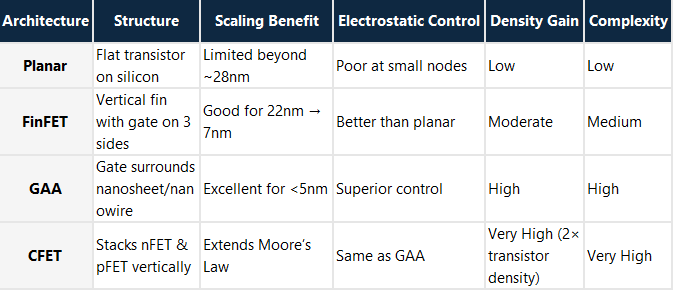
Beyond this, transistor optimisation technologies like FinFET then Gate-All-Around (GAA) provides optimisations in transistor density and lessens voltage leakage across the gates by surrounding the channel on all sides.
And as all real estate professionals know when you’ve built as much as you can on a piece of land and you’ve used up all your X & Y axis space, the solution is to start building up and scale into the vertical plane, CFET does exactly that by allowing stacking of transistor polarities (nFET & pFET) on top of each other rather than side by side as in GAA, thus essentially doubling the transistor capacity on a die, by adding this ‘2nd floor’. As of Q4 2025 CFET is still in early prototyping phase.
The table and diagram below compares the evolution from Planar → FinFET → GAA → CFET


Trend 2 – Beyond Electrons: The Photonic Future
So that buys a bit more time, but then the bottleneck and limitations start becoming the actual materials themselves, the silicon and the copper wires that the electrons flow along, in the words of Scotty from Star trek ‘Ye cannae change the laws of physics’ so the very materials that are used need to be re-evaluated to maintain the momentum of progression.
Once electrons over copper become power‑limited, the only path left is moving data using photons (light). Photonics eliminates resistive heat, delivers higher reach, and radically reduces power per bit.
So silicon possibly makes way for alternate materials like Graphene, and electrons over copper make way for photonics as the physics of electricity with regards to speed, distance and heat generation start to break down in favour of the properties of light. Manufactures like NVIDIA are already adding photonic capabilities into chips like the Rubin ultra GPU (due for release in 2027) by incorporating Co-Packaged Optic (CPO) modules adjacent to the GPUs.
NVIDIA has also introduced Quantum‑X and Spectrum‑X silicon photonic networking switches, leveraging CPO to overcome the scaling limits of traditional electrical signalling and optical transceivers in large‑scale AI deployments.
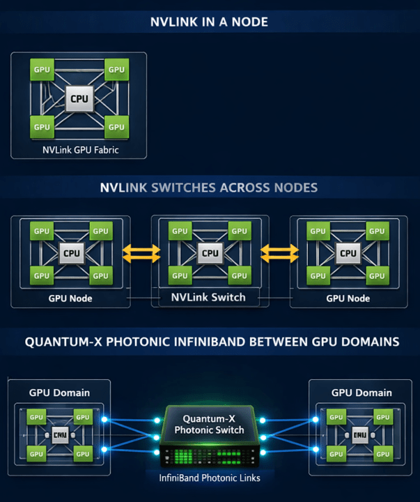
So what role do these photonic switches play? Well lets have a quick review of how GPUs interact with each other. At the node level, NVLink provides a high bandwidth, low latency mesh that connects GPUs (and CPUs) inside a single system, enabling very fast peer‑to‑peer communication and collective operations.
For systems designed for a distributed NVLink domain like, NVIDIAs NVLxxx systems, NVLink Switches extend this fabric to interconnect GPUs across multiple nodes in a rack to ‘Scale up‘ the GPU domain, creating a single, unified ‘GPU domain’ with coherent, all‑to‑all connectivity, allowing massive configurations like NVIDIA’s NVL576 where 576 Rubin ultra GPUs behave as one giant accelerator domain in a single Kyber rack.
Beyond rack scale, NVIDIA’s Quantum‑X Photonic InfiniBand switches provide photonic enabled ‘scale‑out‘ networking that links these NVLink GPU domains together across multiple racks. By integrating silicon photonics directly into the switch ASIC with CPO, Quantum-X reduces power consumption, improves signal integrity, and enables orders‑of‑magnitude scalability for multi‑rack AI fabrics compared with traditional electrical or pluggable optical approaches.

Likewise, Spectrum‑X Photonic switches bring the same CPO‑based silicon photonics to Ethernet networking, enabling cost and power efficient connectivity for AI “factories” comprised of millions of GPUs. The shift from electrical signalling and discrete optics to co‑packaged photonics is critical as AI clusters grow beyond what copper or classic optics can efficiently support
Trend 3 – Beyond Classical: The Quantum Horizon
And what about the ‘double whammy’ I mentioned above well that obviously requires a paradigm shift in computing which takes the form of Quantum computing which is no longer science fiction as Quantum computers are already with us with chips like ‘Willow’ from Google.
One of my previous blog posts was on possible options of how we can reduce the power requirements of AI, one of which was ‘Ternary computing’ where we use ‘Trits’ instead of ‘bits’ where a ‘bit ‘can have 3 states rather than the binary 2, thus giving 50% more information in every ‘Trit’. But Quantum takes that to the next level where each bit or ‘qubit’ can be a 1 or 0 at the same time.
Now that sounds an impossible concept . but how it was explained to me which kind of made sense, is think of a bit which can have 2 states, like a coin, it can be ‘heads’ or ‘tails’ but if you flip that coin in the air while it is spinning it can be said to be both ‘heads and tails’ or in Quantum terms is in ‘Superposition’ these qubits attach to each other via a process called ‘Entanglement’ which then allow processing to evaluate all possible outcomes simultaneously, as every combination can be evaluated in parallel due to the Superposition of all the qubits. Now it should be said that Quantum isn’t the answer to ‘life the universe and everything’ that, as we all know is 42,, and you are certainly not going to run Windows on it, but it does meet a very specific requirement when it comes to the fundamentals of linear equations like complex addition and multiplication functions, and that is where quantum absolutely leaves traditional compute in the dust.
This has obviously caused concern that encryption methods like RSA and ECC while nigh on impossible to break with conventional computing power, could be broken quite easily with the simultaneous evaluation properties of quantum. The day when all widely used public-key encryption methods could be vulnerable to commercially available quantum computing has been named ‘q day’ and could be as close as 2030 hence why many vendors are now offering post-quantum cryptography PQC solutions.
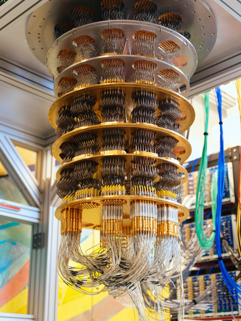
Quantum infrastructure is very different from the infrastructure we are used to with Silicon and copper , instead using materials like Aluminum (Al) or Niobium (Nb) and look more like chandeliers than computers.

These three trends form a pipeline of innovation: more silicon efficiency today, photonics to scale tomorrow, and quantum for the problems classical compute can’t touch
So the answer to the question at the top of this post ‘what’s next for AI Infrastructure’, is ultimately a combination of them all! with ‘Quantum AI’ for specific workloads which will no doubt compliment more traditional enterprise grade AI , with several pit stops along the way utilising the various other technologies mentioned in this post.
As always exciting times ahead.
If you are exploring how to turn AI into something real, not just hype, I’ll be diving deeper into the various vendor solutions I see, architectures and deployment patterns that are actually working in practice, and yes I’m sure our friend Cisco UCS will be featuring in some of them. So follow along if you want straight talk on what delivers outcomes versus what just sounds impressive. More to come at www.ucsguru.com.